
Ai Content Generator
Ai Picture
Tell Your Story

What’s Driving Growth in the Semiconductor Defect Inspection Equipment Market?
Unlocking the Future of the Semiconductor Defect Inspection Equipment Market: Key Growth Drivers and Challenges Ahead
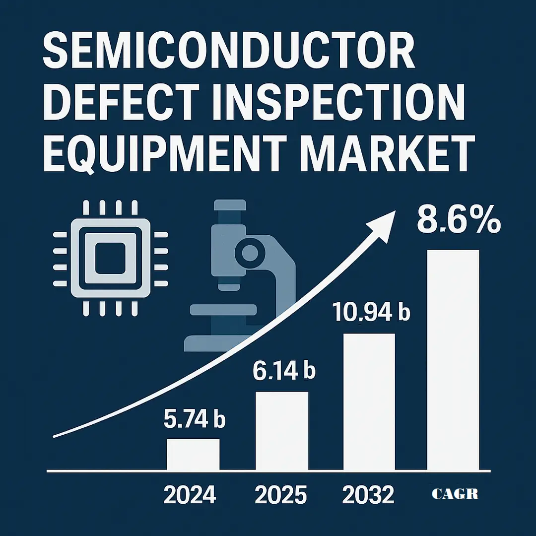
The Semiconductor Defect Inspection Equipment market is experiencing a dynamic shift, powered by innovation, evolving customer expectations, and increasing global integration. As industries across the board seek smarter, more efficient solutions, Semiconductor Defect Inspection Equipment is stepping into the spotlight—reshaping how products are developed, delivered, and deployed.
What’s Fueling the Market Growth?
Several factors are propelling this market forward. First and foremost is the continuous wave of technological innovation, which is enabling faster production cycles, enhanced performance, and smarter automation. Companies are investing heavily in R&D and strategic partnerships, accelerating product advancements and opening up new application areas.
Get a Free Sample Research PDF: https://www.fortunebusinessinsights.com/enquiry/request-sample-pdf/112314
Another key driver is the surge in cross-industry adoption. From manufacturing and energy to transportation and consumer tech, Semiconductor Defect Inspection Equipment solutions are becoming integral to operations, driving productivity, and enhancing competitiveness. As global digitization trends take hold, the demand for scalable, flexible, and efficient Semiconductor Defect Inspection Equipment systems continues to rise.
But It’s Not All Smooth Sailing
Despite its promising outlook, the market faces a few serious hurdles. Complex regulatory environments, particularly in regions with strict compliance mandates, can slow down deployment. Add to that volatile raw material prices and persistent supply chain bottlenecks, and it’s clear that market players need strong strategies and agile operations to stay ahead.
Businesses that can navigate these challenges—by adopting resilient sourcing models and maintaining compliance—are likely to emerge as market leaders in the years ahead.
List of Top Semiconductor Defect Inspection Equipment Market Comapanies:
- KLA Corporation (U.S.)
- Applied Materials (U.S.)
- ASML Holding (Netherlands)
- Onto Innovations Inc (U.S.)
- JEOL Ltd (Japan)
- Lasertech Corporation (Japan)
- NIKON (Japan)
- Veeco Instruments Inc (U.S.)
- Hitachi High Technologies Corporation (Japan)
- Screen Holdings Co. Ltd (Japan)
- Onto Innovation (U.S.)
- Olympus Corporation (Japan)
- Microtronic Inc (U.S.)
- Naura Technology Group (China)
- Bruker Corporation (U.S.)
- Nova Measuring Instruments Ltd (Israel)
Semiconductor Defect Inspection Equipment Industry Devlopments are:
- Onto Innovations Inc. acquired Lumina Instruments Inc., based in Milpitas, California, U.S., and deals in semiconductor wafer defect inspection equipment. The acquisition was done for around USD 250 million. The main purpose of the acquisition was to improve the production capacity of inspection equipment.
- Lasertech Corporation launched a new SICA 108 semiconductor wafer inspection and review system for the semiconductor market. It has features such as high speed in operation and high sensitivity, and it is enabled with smart technologies such as automated guided vehicles and overhead hoist transports.
- Hitachi High-Tech Corporation launched a new DI2800 defect inspection equipment. It is a cutting-edge metrology system that can support semiconductor wafers upto 8 inches (200 mm). It offers features such as ensuring safety and high speed of operation.
- KLA Corporation introduced a new Voyager 1035 defect inspection equipment for the semiconductor market. It uses a DefectWise deep learning algorithm to detect defects and improve the inspection capacity by 30%. This machine is used in the inspection of photoresist layers in applications such as developing inspection and photocell monitoring devices.
- Applied Material Inc. launched a new Cold Field Emission defect inspection equipment that can support the e-beam system and can operate under 1,5000 C. The company launched the SEMVISISION G10 defect review system and Primevision 10 defect inspection equipment for semiconductors and related markets. It has features that are 10 times faster than other inspection systems.
Connect with Our Expert for any Queries: https://www.fortunebusinessinsights.com/enquiry/speak-to-analyst/112314
Key Highlights of Semiconductor Defect Inspection Equipment Market Research Report:
- Comprehensive analysis of the Semiconductor Defect Inspection Equipment Market.
- Identification of market size and growth trends.
- Competitive landscape assessment, including key players and their strategies.
- Consumer behavior insights related to Semiconductor Defect Inspection Equipment usage.
- Emerging trends and opportunities in the Semiconductor Defect Inspection Equipment Market.
- Regional analysis, highlighting variations in Semiconductor Defect Inspection Equipment usage and competition.
- Industry best practices for effective Semiconductor Defect Inspection Equipment optimization.
- Future outlook and market projections for informed decision-making.
The report also explores key limitations and the regional footprint of the industry, both of which could shape future market dynamics beyond 2032. This market analysis is designed to offer a clear and in-depth view of the industry's potential, equipping businesses with the insights they need for strategic decision-making. Packed with over 100 pages, the Semiconductor Defect Inspection Equipment Report features a detailed table of contents, along with numerous figures, tables, and charts that support a thorough evaluation.
Semiconductor Defect Inspection Equipment Market Key Drives:
Drivers:
- Rising complexity in chip designs increases need for precision inspection.
- Surge in semiconductor manufacturing for AI, IoT, and 5G technologies.
Restraints:
- High capital and operational cost of inspection equipment.
- Technological obsolescence due to rapid advancements.
Opportunities:
- Growing demand for defect-free wafers in advanced node technologies.
- Automation and AI integration in defect detection systems.
Table of Contents:
- Introduction 2025
- Research Scope
- Market Segmentation
- Research Methodology
- Definitions and Assumptions
- Executive Summary 2025
- Market Dynamics 2025
- Market Drivers
- Market Restraints
- Market Opportunities
- Key Insights 2025
- Key Industry Developments – Merger, Acquisitions, and Partnerships
- Porter’s Five Forces Analysis
- SWOT Analysis
- Technological Developments
- Value Chain Analysis
TOC Continued…!
Scope of Semiconductor Defect Inspection Equipment Market Report:
The Semiconductor Defect Inspection Equipment Market Report offers an in-depth look at the current state of the industry, highlighting key trends, growth drivers, and existing challenges. It provides detailed insights into market segmentation based on product types, applications, and geographic regions. The report also sheds light on leading companies, their competitive strategies, and emerging opportunities for growth. Additionally, it explores consumer behavior and preferences that are shaping market trends. Backed by solid data, the report delivers forecasts for market size and future growth. It also takes into account regulatory developments and technological advancements, making it a valuable guide for businesses aiming to make strategic and informed decisions.
Request Here for Customization: https://www.fortunebusinessinsights.com/enquiry/customization/112314
About Us:
Fortune Business Insights provides expert corporate analysis and accurate data to help organizations of all sizes make timely decisions. We tailor innovative solutions for our clients, assisting them in addressing challenges unique to their businesses. Our goal is to empower our clients with holistic market intelligence, providing a granular overview of the market they operate in.
Contact Information:
- U.S.: US +1 833 909 2966 (Toll Free)
- UK: +44 808 502 0280 (Toll Free)
- APAC: +91 744 740 1245
- Email: sales@fortunebusinessinsights.com
Related Posts
© 2025 Invastor. All Rights Reserved
User Comments